The RJM Audio B-board
A simple, versatile buffer stage. Its a unity-gain pre-amplifer, a line driver, or a recording buffer. You need this, even if you don't realize it yet!
Buffers make everything better...
In audio, a buffer is the name of a circuit block with a voltage gain of unity (0 dB), a high impedance input, and a high current, low impedance output. Although the current drive is usually the headline feature, when used open loop a buffer also isolates the high negative feedback voltage gain elements of an audio circuit from the difficult to drive, and potentially instability-inducing, capacitance and inductance of a complex load such as a long length of interconnect cable or a pair of headphones, to give the most common examples.

Buffers have obtained a bit of bad reputation over the years as being worse than useless: buffers, it is said, not only provide no signal gain, they also add noise and distortion to the signal! As is often the case, there is a kernel of truth to this wrapped in layers of disinformation: Yes, all buffers add noise and distortion to the signal, but any competently designed buffer is going to add far less noise and distortion than the voltage gain stage that precedes it. A good buffer is for all intents and purposes transparent, or at least more transparent than if the voltage gain stage was driving the load directly.
The Circuit
The basic diamond buffer circuit - generally traced to the National Semiconductor LH0002 - consists of two pairs of complementary transistors arranged in crosswise-symmetry, giving the schematic a diamond shape from which the name derives. Dozens of more complicated variations have appeared, the B-board circuit is taken from a more recent application note for current amplifiers and is pretty much identical to the original except that damping resistors are added to the base of each transistor.

Texas Instruments literature number SNOA365c.
Filleting the buffer out of the current op amp feedback loop shown above, and adding an extra resistor for output overcurrent protection and extra isolation, we get the following circuit:
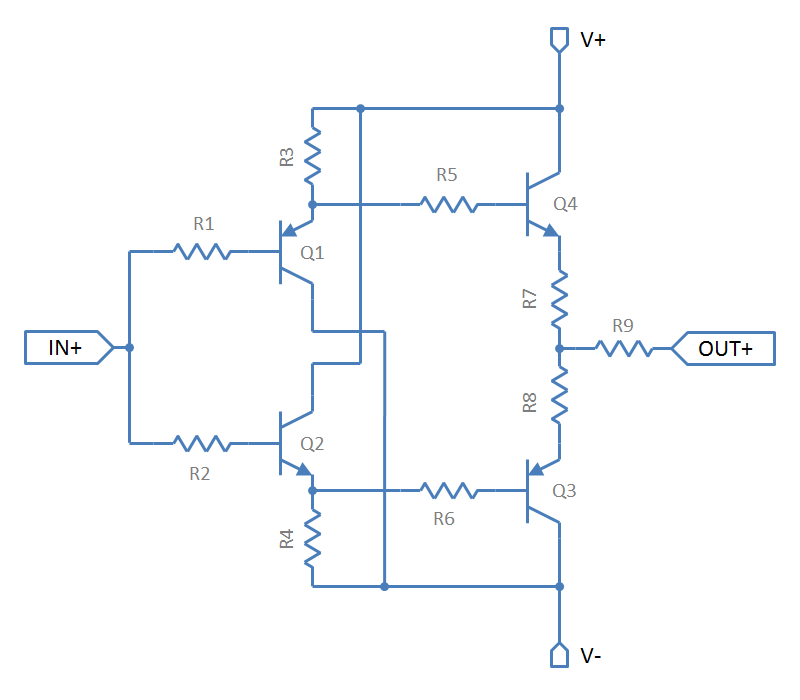
The B-board diamond buffer circuit.
In the classic diamond buffer configuration, Q1 and Q3 are identical devices, as are Q2 and Q4. All four transistors operate at the same bias current. Inefficient, yes, but all that symmetry results in exceptionally low distortion.
The buffer circuit requires split supplies. A diamond buffer has a high power supply rejection ratio, and line level audio is not especially sensitive to ripple anyway, but it's probably a good idea to install some voltage regulation. For this we turn to the simple-yet-suprisingly-effective "zener regulator with series pass transistor" circuit, which I call the Z-reg:
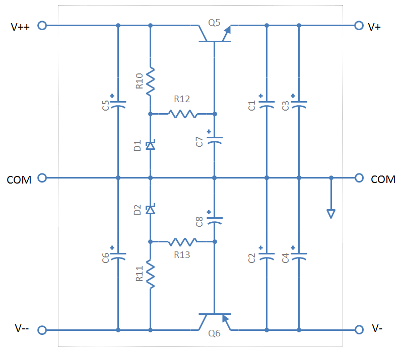
The B-board Z-reg circuit.
The Z-reg uses Zener diodes D1 and D2 to provide the reference voltage, filters that, and feeds the result to the base of the pass transistors Q5 and Q6. The output voltage, taken from the emitter of the pass device, remains nearly constant at one diode drop below the Zener voltage. Wide effective bandwidth, no feedback. For line level circuits, this is all the voltage regulation you need. For low level signals like phono stages and mic preamps, consider the X-reg instead.
Normally the B-board shares the power supply in common with the rest of the electronics in the box, but, when used independently, it can be powered from a 2x12 V, 25 VA toroid transformer and bridge rectifier combination as shown:
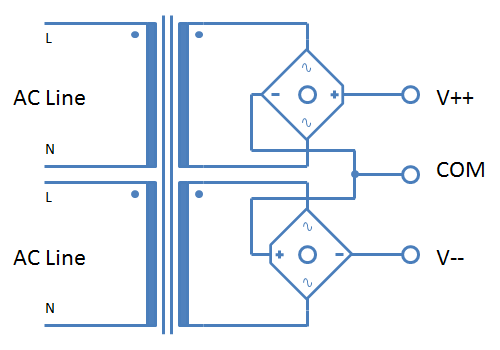
The B-board unregulated power supply.
One power supply is typically shared between two channels, but of course dual mono operation is also possible.
Component List
Line driver configuration shown:
| Component | Value | Description |
|---|---|---|
| R1,2 | 47R | 1/2 W |
| R3,4 | 1k | 1/2 W |
| R5,6 | 47R | 1/2 W |
| R7,8 | 1R | 1/2 W |
| R9 | 47R | 1/2 W |
| R10-11 | 1k | 1/2 W |
| R12-13 | 1k | 1/2 W |
| C1-4,7,8 | 100µ | 25 V, 5 mm lead spacing, Nichicon FW or KW. |
| C5,6 | 1000µ | 25 V, 3.5 mm lead spacing, Nichicon FW or KW. |
| D1,2 | 12V | 0.5W Zener Diode |
| Q1,3,5 | BD135 | NPN transistor |
| Q2,3,6 | BD136 | PNP transistor(ECB pinout.) |
| T | 2x12VAC | 25VA toroid transformer. |
| BR | 3A 200V | Two per power supply. |
The emphasis is on cheap, widely available, and highly substitutable parts. The exact parts and values are really not critical. A more comprehensive parts list and worksheet is found in the BOM.
The Layout
I have designed circuit boards for this project. Actually this project was all about the layout and circuit boards, as the circuit itself is trivial. The Eagle board and schematic files are available to download. Usual "free for personal use, no commercial gain" condition applies.The boards are small and narrow, 10 x 4 cm, designed to get into the tight spaces often encountered when retrofitting exsisting equipment. The connections are straightforward enough, with the signals together on the bottom, and the power connections on the left and right sides.

Three things about the connections:
- The GND connects the circuit common to the chassis, it should only be used when there is no other such connection made anywhere else for that particular channel. For example, if you are using the B-board paired with the Phonoclone 3 boards, which also have a GND connection, the chassis connection is made at the Phonoclone 3 board, only.
- There are two sets of power connections, and they work slightly differently depending on how the board is used. In the normal case the on-board Z-reg regulator is used, and the board hooked up to the unregulated power supply through the left side connections V++, COM , V--. In this scenario the right side connections V+, COM , V- become outputs allowing other circuit elements to be powered from the Z-reg regulated voltage. If, however, you do not want to use the Z-reg, then leave the Z-reg part of the board unpopulated (everything to the left of R3 on the board, shown above) and power the board by an external regulated supply hooked up to V+, COM , V-.
- IN+ must be connected to IN- by an resistance equal to 100k or less. Since this resistor is normally part of the previous stage I have not included it on the board or the circuit schematic, but please understand the B-board will not work properly with the inputs floating. (Be sure to short the inputs when testing the board on the bench.)
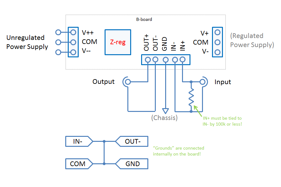
Board block diagram and connections.
Construction Notes
Q. Where can I use the B-board?
A. Just about anywhere.
It's a output stage for source components. The original application was to buffer the VSPS and Phonoclone phono stages. The boards are placed next to the phono stage boards, and powered from the same supply. The photo stage output would be routed though the buffer and the output of the buffer connected to the output RCA jacks. In a similar vein the B-board can be used with any line level source component, phono stage, mic preamp, or DAC.
It's a pre-amplifier. Combined with a volume attenuator and input switches, it is a unity gain active pre-amplfier. With an additional voltage gain stage powered by the Z-reg outputs, it becomes a full-fledged pre-amplifier.
It's a recording loop buffer. Tape outputs seem a bit archaic these days, but the B-boards can be used in this capacity.
rjm003.geo at yahoo.com