The J-Mo Mk. II Headphone Amplifier
Party like it's 1999. Again.

This is a followup to the JFET-MOSFET headphone driver project. That circuit has the distinction of being the first one I actually designed myself, way back in, you guessed, 1999. Neither elegant nor innovative, it is filled with the hedonistic spirit of that crazy millenium year. I have a fondness for it.
Chalk it up to nostalgia perhaps. It wasn't even a circuit that make much sense, I mean, a choke regulated power supply with 48,000 µF of filter capacitance for a headphone amplifier?? Somehow though, in 1999, against the backdrop of reading Sound Practices magazine, Harvey "Gizmo" Rosenberg's ramblings, and tube-era electronics textbooks it didn't seem at all odd. DIY audio back then wasn't about making sense, it was about trying out whatever crazy idea sprang to mind, the crazier and more outlandish, the better.
I still think the single-ended MOSFET source follower has merit though. Zero-gain headphone buffers taking up a full width 1U chassis - not so much. The original circuit could use some strategic re-working to trim some of that end-of-century excess. While we are at it, some voltage gain would be nice...
So with a new nickname, the "J-Mo" and under a "Mk. II" badge, the JFET-MOSFET headphone driver gets a twenty-first century update.
The Design Parameters
The J-Mo Mk. II is configured for 100 mW class A output into 16-65 ohm loads. A JFET and NPN transistor arranged as a Sziklai pair provide voltage gain of about 10 dB and drive the MOSFET source follower, which runs open loop. Total circuit power consumption per amplifier channel is about 3 W. Channeling Harvey Rosenberg a little, what we are embarking on here is a brute force extraction of audio tonality. Efficiency is not even in the picture. This one is going to be played by our rules, old school.
Where have all the JFETs gone?
The original J-Mo used a 2N4416 metal-can JFET for the input stage. It is no longer widely available. The ranks of JFET parts, especially in through-hole packages, have been decimated. As many of the remaining parts are marked "end-of-life" choosing a JFET that will likely still be around in five years is a problem. While the choice of JFET is not critical, the resistance values do have to be tweaked slightly when a different JFET is substituted. It would be nice, therefore, to pick a model that is destined for wide and long-lived availability. For the new circuit to work optimally with a gain of 3, we need a mid-sized JFET with IDSS averaging around 8-12 mA. We select the 2N5486.
The original design called for an IRF510 MOSFET. This part is still current and widely available, and careful searching did not turn up anything in through-hole packaging that would be an obvious improvement. So we will stick with the IRF510 as the output device.
The Amplifier Circuit

The J-Mo Mk. II circuit, one channel shown.
The JFET and transistor are in a Sziklai pair feedback configuration, which, with the insertion of the 1.5 kohm resistor between the BD136 collector and JFET source, provides reliable gains above unity and decent output drive. The Sziklai circuit has a large large DC output voltage that we use to bias the MOSFET gate. The 1k trimmer resistor is adjusted until the voltage on the MOSFET source is equal to 5.5 V. Note that it is important to match the JFETs reasonably closely.
Devices shown boxed in red will get hot. The source resistor should be at least a 2W type, and a small but decent heatsink is needed for the MOSFET. A thermal resistance of about 10 C/W should be sufficient. A vented case as advised.
JFET inputs, capacitively-coupled, singled-ended circuit, and low voltage, single-supply operation make this amp pretty much bullet proof. Apart from matching the JFETs, it is simple to build and very tolerant, with benign clipping and a very natural distortion signature. It also has plenty of power reserve. It's a bit of a cliche, but yeah, with 100 mW on tap this amplifier will pretty much drive any low to mid impedance headphone you care to throw at it.
Component List
See the circuit schematic for the component numbering scheme.
| Component | Value | Description |
|---|---|---|
| R0 | 20k | Logarithmic stereo volume control. |
| R1 | 100k | |
| R2 | 470R | |
| R3 | 1k5 | |
| R4 | 47R | |
| R5 | 1k trim | 10 turn linear trim potentiometer |
| R6 | 47R | |
| R7 | 30R | 2 W power resistor |
| R8 | 100k | |
| R9 | 47R | |
| C1,2 | 1000µ | 25 V, 5 mm lead spacing, Nichicon FW or KW. |
| C3,4 | 100µ | 25 V, 3.5 mm lead spacing, Nichicon FW or KW. |
| Q1 | 2N5486 | n-channel JFET |
| Q2 | BD136 | pnp transistor |
| Q3 | IRF510 | n-channel MOSFET |
Only Q1 needs to be matched, and it doesn't need to be that close. Using a 2k2 source resistor, apply +16 V (for example) to the drain and measure the source-gate voltage. Try and use pairs that give Vgs voltages within 10% of each other. From 5-10 devices you should get several good pairs.

A more comprehensive parts list is found in the BOM. (Zipped Excel .xlsx format.)
The Circuit Board
8x5 cm, dual mono, dual-sided circuit boards have been designed for this project. The boards do not include the voltage regulator circuitry, just the amplifier. The boards connect to a 15-18 V regulated supply.

The J-Mo Mk. II headphone amplifier board, one channel shown.
Full circuit schematic (from the Eagle board files, parts values are representative, consult BOM for exact values.)
Download Eagle Files (Download BOM)
Boards and parts are available, see the products page page for details.
Voltage Regulation and Power Supply
The amplifier is powered by a 15-18 V regulated supply. Each channel draws about 200 mA. To be on the safe side, I recommend that the supply be rated for 1 A. You can use whatever you have lying around.
Here is the "complimentary" 16 V, 200 mA power supply designed to power one J-Mo Mk. II channel. It is a series regulator with Zener voltage references and an IRF510 as the pass element. It's what I'd use.

The J-Mo Mk. II regulated power supply circuit.
Four 10V Zener diodes are used, the reference is 20 V created by two zeners in series. The second Zener stack protects the MOSFET gate from voltage transients during shut down. The filtered Zener reference and IRF510 do a good job or reducing the ripple, but the final result would still be a bit too high without the extra 10 ohm resistor and 1000 µF capacitor forming an RC filter stage on the input. With this assistance, the output ripple drops down below 1 mV for 200 mA output. The amplifier circuit mops up the rest.
The AC line components are not shown in detail. The power supply chassis is normally connected to earth for safety, and the AC line is fused with a 1 A slow-blow fuse. The power supply can be in the same chassis as the amplifier circuit. I recommend the Triad Magnetics 100 VA toroid (VPT36-2780) with two 18 VAC secondaries. One secondary winding powers the left channel diodes and regulator, the other secondary winding powers the right channel. Good channel isolation without the bulk and expense of two power transformers.
The Circuit Board
The regulator circuit is a 8x5 cm, dual mono, dual-sided circuit board designed to match the main amplifier.
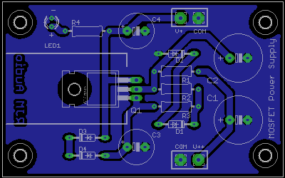
The J-Mo Mk. II mosfet voltage regulator board, one channel shown.