CrystalFET Phono Stage
Passive two stage design, in the JFET-as-tubes-paradigm.
Postscript: Achieving 60 dB in a two stage passive phono circuit requires 40 dB from each amplifier stage. This proved to be a bridge too far for the J113 JFETs used. Ultimately this design is therefore best suited as an MM phono stage.
A phono stage for moving magnet or moving coil cartridges with the following features:
- Accurate RIAA equalization obtained using common, standard value capacitors.
- Switch between moving coil and moving magnet gain setting of 56 dB and 35 dB (approx.).
- Very low power consumption.
- All jfet amplifier topology.
The two stage passive RIAA phono stage is a classic circuit of diy audio. I built one a long time ago with 6DJ8 tubes. The conceptually simple and easy-to-follow circuit - two gain stages bracketing a passive filter - makes it popular with beginners, and variants using tubes, jfets, and op amps for the gain stage can be found. Come to think of it, I've done the op amp version too.
While the op amp version has its own issues, the jfet and tube versions are actually much harder to pull off. The simplicity of the circuit is misleading. In essence it's just passing the buck over to the power supply. Whereas most circuits are designed to block power supply noise from the output, this circuit actually amplifies power supply noise into the output signal. The power supply must therefore be exceptionally low noise.
The Amplifier Circuit
Jfets have high input impedance and relatively low noise, but limited drive capacity - at least when configured as a common source amplifier. What I have chosen to do, therefore, is buffer each amplifier stage with a second jfet configured as a source follower. As a gain block, the combination increasing the drive capacity significantly. The impedance of the RIAA filter network can be reduced, making it less noisy, while the output stage can drive interconnect cables and moderately low impedance loads.

The main complication are the jfet amplifiers. Long story short is the jfets come from the factory all slightly different, and for this circuit to work properly the jfets need to be the same. So each jfet must be measured, binned, and matched to a parameter called the pinch-off voltage which for the J113 jfet varies between -0.5 and -3.0 V. The crystalFET requires Q1 and Q3 to be matched between channels and have pinch off voltages about -1.3 to -1.7 V. Q2 and Q4 don't need to me matched.
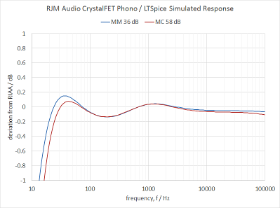
As seen in the simulation, the RIAA response of the circuit is accurate to within 0.2 dB.
The Power Supply
As noted earlier, the power supply is where most of the design effort went. The voltage regulator is based on two p-channel MOSFETs, Q7 configured as a current source, Q8 as a voltage amplifier that acts as the current shunt element. With the CRC filter stages R14-16 included the power supply the ripple rejection of the regulator stage is below 120 dB at 120 Hz. It is sufficient to remove all traces of ripple from the measured output noise.

The voltage regulator is fed from a rectified 30 VAC secondary winding.
Construction Notes
The voltage regulation and filtering is placed on the same board as the phono circuit. The power transformer and rectifier diodes are typically in a separate chassis connected by an umbilical cable.
rjm003.geo at yahoo.com